
Great Lakes

Friday, January 25, 2013
Artistic PCB Boards with a script
I love beautifully created traces on a PCB board. It appears that others are with me. I saw this post from someone who has wrote a program to artistically render traces. It may not be practical for a lot of the dense designs we all work on, but I could definitely see this as useful for simpler board stackups with simple routing. Here is a snapshot of the boards and a link to the article: link.

NFC and The Future
Have you been hearing about Near Field Communications, more popularly referred to as NFC? NFC is a superset of RFID that runs at 13.56 MHz. The unique differentiation between NFC and RFID is that NFC silicon chips can communicate in three different ways:
1.) Read/Writer to Tag mode - This is the traditional use case of RFID where you have a reader/writer chip that reads a tag, most often a badge. You see this type of implementation all the time in security access systems.
2.) Tag emulation mode - This is the mode where the silicon device can emulate a traditional tag. So now you could use an NFC enabled phone as your security access to get in the building instead of having to also carry a badge.
3.) Peer to Peer mode - This is the mode that you see on all the Samsung Galaxy commercials where two people are bumping their phones together to exchange music playlists.
So why am I writing about NFC? Well, for one Avnet has great partnerships on this technology with vendors like NXP, TI, ST, Maxim, as well as passive antenna suppliers. Secondly, I am also hoping that we can make this technology more prevalent by having Apple adopt it in its next round of products. Today, Android phones, Android Tablets, and Windows based laptops are shipping with NFC technology enabled.
So before I wrap up, I wanted to highlight a few reasons why you might want to consider NFC for your next device:
1.) Enablement - With cellphones, tablets, and laptops having this feature you can integorrate your products in a straight-forward manner.
2.) Low Power - You can use the energy of the 13.56MHz antennna and power your NFC enablement compeltely through the phone, tablet, laptop.
3.) Short Range - There is a short range (Few cms), but I am finding this is sufficient for most applications. If you need to program your device through packaging or in an enclosure, I have showcased the range to be suitable for NFC.
That's all for now! Have a great Friday!
-Jason
Thursday, January 17, 2013
The Offspring of Fairchild Camera and Instrument
In my family, our lineage was taught to me at a young age. It made it easy to memorize my lineage because a large portion of my family occupies the same cemetery. In addition, my dad has spent a lot of time tracing my ancestors on his side and educating me about our ancestry. I have always had an interest in genealogy and so I was pleasantly surprised when I found the family tree from Fairchild Camera and Instrument. I wanted to repost this article from DSP Related so that you can see what great companies spawned from Fairchild Camera and Instrument:
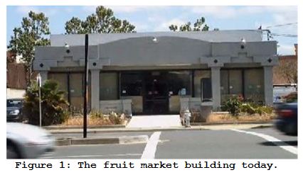
There used to be a fruit market located at 391 San Antonio Road in Mountain View, California. In the 1990's I worked part time in Mountain View and drove past this market's building, shown in Figure 1, many times, unaware of its history. What happened at that fruit market has changed the lives of almost everyone on our planet. Here's the story.
 William Shockley
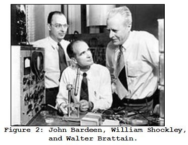
In 1948 the brilliant physicist William Shockley, along with John Bardeen and Walter Brattain, co-invented the transistor at Bell Laboratories in New Jersey. (Justifiably they were awarded Nobel Prizes in Physics in 1956.)
 In 1955, deciding to move back to where he grew up, Shockley returned
to California. He wanted to start his own company to commercialize
semiconductor devices. Joining a college friend's successful company,
Beckman Instruments, Shockley was appointed Director of Beckman's newly
founded Shockley Semiconductor Laboratory division which bought the old
fruit market at 391 San Antonio.
In 1955, deciding to move back to where he grew up, Shockley returned
to California. He wanted to start his own company to commercialize
semiconductor devices. Joining a college friend's successful company,
Beckman Instruments, Shockley was appointed Director of Beckman's newly
founded Shockley Semiconductor Laboratory division which bought the old
fruit market at 391 San Antonio.
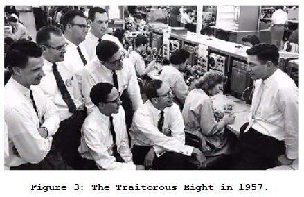
Shockley, who was nationally famous in the field of electronics at that time recruited the best and brightest scientists and engineers to work at his Shockley Semiconductor Laboratory. However, his domineering management style, bizarre behavior that bordered on paranoia, and his loss of interest in developing commercial transistors and integrated circuits caused eight employees to leave Shockley Labs. That was on Sept. 18, 1957, a day that was ranked by the New York Times newspaper as one of the Top 10 Days That Changed the World.
Traitorous Eight
Those "Traitorous Eight", as Shockley called them, wanted to start their own semiconductor company. (Those engineers are shown in Figure 3. And yes, engineers really did dress that way in the late 1950s.)
 Intrigued by these new-fangled transistors, New York industrialist
Sherman Fairchild agreed to finance The Traitorous Eight by creating a
new company called Fairchild Camera and Instrument. It was at Fairchild
that the first commercially-viable integrated circuit was invented. From
that single company evolved the greatest collection of semiconductors
companies in the world, as well as a California location that came to be
known as "Silicon Valley." Figure 4 gives you some idea of the
astounding commercial outgrowth of Fairchild Camera and Instrument.
Intrigued by these new-fangled transistors, New York industrialist
Sherman Fairchild agreed to finance The Traitorous Eight by creating a
new company called Fairchild Camera and Instrument. It was at Fairchild
that the first commercially-viable integrated circuit was invented. From
that single company evolved the greatest collection of semiconductors
companies in the world, as well as a California location that came to be
known as "Silicon Valley." Figure 4 gives you some idea of the
astounding commercial outgrowth of Fairchild Camera and Instrument.
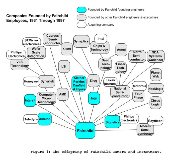 (Figure 4 is a redrawn, without permission, version of a graphic
found on page 12 of the in October 2007 issue of The IEEE Spectrum
magazine. A more informative version of Figure 4 is available at http://www.businessweek.com/pdfs/fairkid.pdf.)
(Figure 4 is a redrawn, without permission, version of a graphic
found on page 12 of the in October 2007 issue of The IEEE Spectrum
magazine. A more informative version of Figure 4 is available at http://www.businessweek.com/pdfs/fairkid.pdf.)
The venture capital firm of Kleiner, Perkins, Caufield & Byers is included in Figure 4 because they provided financial backing for many electronic and information technology startup companies. You may have heard of some of those companies; Amazon, Google, Sun Microsystems, AOL, Compaq, Electronic Arts, Intuit, Netscape, and others.
Transistors, They're Everywhere
Roughly ten years ago a technologist in the semiconductor industry estimated that mankind produces more transistors annually than grains of rice. That estimate is not as far-fetched as it might seem. In reference [2] the authors stated:
Transistors do indeed seem to be nearly everywhere in our modern lives. I walked around the rooms of my 1500 ft2 house and realized that no matter where I stood I was never more than 3 meters from a semiconductor device. (On my bathroom counter resides a battery powered tooth brush, sitting in its recharging base.) I finally stood at the far end of my garage away from the corner where my clothes washer is located, thinking that was a spot surely more than 3 meters from a transistor. Then I realized that on the outside of the garage wall, next to where I was standing, is my electric utility company’s Smart Meter with its RF transmitter circuitry.
The inventions of the transistor and the integrated circuit (interconnected transistors) have literally transformed our world--from singing greeting cards to iPads, from home computers to interplanetary spacecraft. There is no way to overstate the importance of the technology that blossomed from that little fruit market at 391 San Antonio Road.
The Little Fruit Market
Posted by Rick Lyons on Jan 14 2013There used to be a fruit market located at 391 San Antonio Road in Mountain View, California. In the 1990's I worked part time in Mountain View and drove past this market's building, shown in Figure 1, many times, unaware of its history. What happened at that fruit market has changed the lives of almost everyone on our planet. Here's the story.
In 1948 the brilliant physicist William Shockley, along with John Bardeen and Walter Brattain, co-invented the transistor at Bell Laboratories in New Jersey. (Justifiably they were awarded Nobel Prizes in Physics in 1956.)
Shockley, who was nationally famous in the field of electronics at that time recruited the best and brightest scientists and engineers to work at his Shockley Semiconductor Laboratory. However, his domineering management style, bizarre behavior that bordered on paranoia, and his loss of interest in developing commercial transistors and integrated circuits caused eight employees to leave Shockley Labs. That was on Sept. 18, 1957, a day that was ranked by the New York Times newspaper as one of the Top 10 Days That Changed the World.
Traitorous Eight
Those "Traitorous Eight", as Shockley called them, wanted to start their own semiconductor company. (Those engineers are shown in Figure 3. And yes, engineers really did dress that way in the late 1950s.)
The venture capital firm of Kleiner, Perkins, Caufield & Byers is included in Figure 4 because they provided financial backing for many electronic and information technology startup companies. You may have heard of some of those companies; Amazon, Google, Sun Microsystems, AOL, Compaq, Electronic Arts, Intuit, Netscape, and others.
Transistors, They're Everywhere
Roughly ten years ago a technologist in the semiconductor industry estimated that mankind produces more transistors annually than grains of rice. That estimate is not as far-fetched as it might seem. In reference [2] the authors stated:
- Semiconductor production has increased by an astounding average of 16% per year for the last forty years.
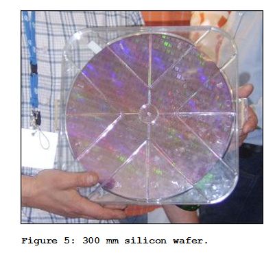
- In 2002 there were more bits of memory on a single 300 millimeter silicon wafer than were produced by the entire semiconductor industry in 1984.
- There were more transistors produced in 2002 than grains of rice, and each rice grain could buy 100's of transistors.
Transistors do indeed seem to be nearly everywhere in our modern lives. I walked around the rooms of my 1500 ft2 house and realized that no matter where I stood I was never more than 3 meters from a semiconductor device. (On my bathroom counter resides a battery powered tooth brush, sitting in its recharging base.) I finally stood at the far end of my garage away from the corner where my clothes washer is located, thinking that was a spot surely more than 3 meters from a transistor. Then I realized that on the outside of the garage wall, next to where I was standing, is my electric utility company’s Smart Meter with its RF transmitter circuitry.
The inventions of the transistor and the integrated circuit (interconnected transistors) have literally transformed our world--from singing greeting cards to iPads, from home computers to interplanetary spacecraft. There is no way to overstate the importance of the technology that blossomed from that little fruit market at 391 San Antonio Road.
Monday, January 14, 2013
TI's WEBENCH Schematic Export
Happy Monday! Although the NFL playoffs didn't go as well as I hoped, at least the bright side is I have my Sundays free again.
I did want to share some news from TI in case you did not see this last year. TI has a tool called WEBENCH that allows to create power topology solutions for your designs. This tool can be used for selecting one power part or going through a complex power topology that might be necessary when powering an FPGA. I have used WEBENCH a lot, and find that it helps me get to the best architecture quicker. It goes through all the power calculations for you and helps you see the tradeoffs of cost, size, and efficiency. At the end of last year, they added a new feature to WEBENCH, schematic export! Now you can go write from design into schematic. They support Altium Designer, OrCad Capture CIS, and the free tool DesignSpark. They are working on support for Mentor DxDesigner and Altium's P-Cad.
Check out the link from TI to learn more!
Friday, January 4, 2013
Top Ten Products from EE Times User Reviews
I love the New Year because we get to look at what was hot in 2012. Here is another list from 2012 from EE Times.
Avnet made the list with our ZedBoard design.
Wednesday, January 2, 2013
It's a New Year - How about a USB Topic
Welcome to 2013! I hope you had a great 2012 and enjoyed your holidays. I took some time off and I am now feeling refreshed and energized to start 2013. I was made aware by a friend today of a bit-banged USB implementation on an MSP430. This is very exciting because the only options of doing this in low cost designs is to add an additional translation chip, usually a USB to uart bridge. For those of you interested in going right to the content, check out this link.
I did want to give a little background on why someone would want a bit-banged USB implementation on a microcontroller. Today USB is the most ubiquitous interface available in the market. The connector was largely driven by the consumer space but has started to adapt quite well to markets I am more familiar with, medical and industrial. Although USB is widely used, it is not the easiest thing to understand. There are numerous profiles that have to be coded in software and different configurations that have to be accounted for in hardware.
Traditionally if a user wants to a add a USB connection they either have to get a processor with a USB controller or they have to insert a USB to UART bridge chip in between their microcontroller and the USB port. There are numerous suppliers with USB to UART bridge chips and the most popular is probably FTDI.
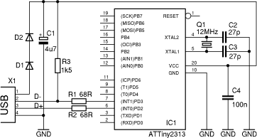
There are numerous open source projects that I am aware of that are starting to implement the bit-banged USB implementation without a bridge chip in between. A very popular implementation is the one for the AVR micros called V-USB - link.
Here is the schematic required to add a USB connection for the V-USB implementation, pretty simple:
I did want to give a little background on why someone would want a bit-banged USB implementation on a microcontroller. Today USB is the most ubiquitous interface available in the market. The connector was largely driven by the consumer space but has started to adapt quite well to markets I am more familiar with, medical and industrial. Although USB is widely used, it is not the easiest thing to understand. There are numerous profiles that have to be coded in software and different configurations that have to be accounted for in hardware.
Traditionally if a user wants to a add a USB connection they either have to get a processor with a USB controller or they have to insert a USB to UART bridge chip in between their microcontroller and the USB port. There are numerous suppliers with USB to UART bridge chips and the most popular is probably FTDI.
There are numerous open source projects that I am aware of that are starting to implement the bit-banged USB implementation without a bridge chip in between. A very popular implementation is the one for the AVR micros called V-USB - link.
Here is the schematic required to add a USB connection for the V-USB implementation, pretty simple:
Subscribe to:
Comments (Atom)